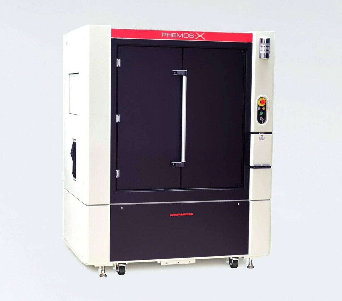
Hamamatsu Photonics has developed a new semiconductor failure analysis system called the “PHEMOS-X C15765-01” that in just a single unit utilizes visible to near-infrared light to analyze semiconductor defects. What makes this possible is a newly mounted multi-wavelength laser scanner that applies our unique in-house optical design technology. Efficiently utilizing multi-wavelength light allows high sensitivity and high resolution essential for localizing semiconductor failures and so will improve failure analysis efficiency in diverse semiconductor devices that will be in high demand, such as state-of-the-art semiconductor devices whose circuit line width keeps on shrinking as well as power semiconductors that control electrical power more efficiently than ordinary semiconductor devices. Sales of the PHEMOS-X start on Thursday, April 1, 2021 for both domestic and overseas semiconductor device manufacturers.
To access the full article please follow the below link: https://www.hamamatsu.com/eu/en/news/product_technology/2020/20201222000000.html
For further information contact us on email: [email protected] or visit our website: www.hamamatsu.com