(25th June 2021, Muellheim, Germany) Often, when the requirement is for geometrically complex, feature-rich, highly precise, and innovative metal parts and components, manufacturers default to stamping. However, micrometal GmbH (incorporating Etchform and HP Etch) has developed unique and proprietary refinements to the photo-chemical etching (PCE) technology that out-rivals traditional metal fabrication processes and traditional PCE processes. micrometal’s PCE process out-competes alternatives in terms of control, accuracy, repeatability, speed, and cost, while at the same time producing parts with no stress-related material degradation or burrs.
PCE not only copes well with difficult geometries, it also allows design engineers enormous flexibility, facilitating the adjustment of designs right up to the point of manufacture due to the use of digital film or glass tooling. Such tooling is hugely less expensive and much faster to produce and alter than the hard steel tools needed for punching and stamping, making the process ideal for prototyping (as well as low, medium, and high volume runs). Also, as the tooling is transferred to metal through a contact printing process, there is no tool wear ensuring that the first part produced is identical to the last. When using stamping, part complexity adds cost, but PCE is unaffected by the level of tool complexity, and it makes no difference in terms of costs or lead-time how complex the geometry of the part is and therefore the complexity of the digital film or glass tooling.
However, micrometal has evolved the already precise PCE technology, and has optimized the process so that today it offers levels of precision and tolerance attainment impossible using traditional PCE or any other more traditional technologies.
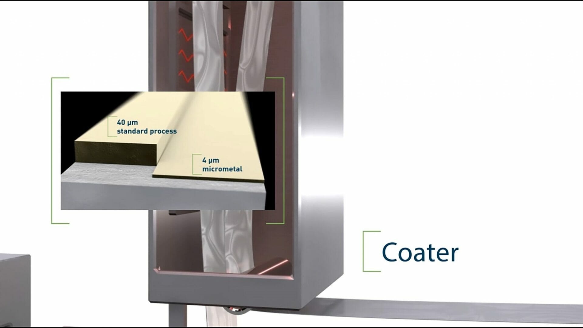
Dr Angel Lopez, Director of Business Development at micrometal says, “There are many stages in the PCE process, and at micrometal we have focused in on a couple in particular to refine the technology to cater for the ever more exacting requirements of our customers throughout industry. micrometal’s PCE process is very different from conventional PCE processes. Uniquely, we use a special liquid resist system to obtain ultra-thin (2-8 micron) photoresist layers enabling a higher degree of precision in the chemical etching process. It allows us to achieve extremely small feature sizes of 25 microns, a minimum hole diameter 80% of the material thickness, and single digit micron tolerances repeatably. In addition, along with our optimised exposure system we can avoid the parallax problems typically associated with PCE.”
Lopez continues, “Traditional PCE uses relatively thick dry film resist which compromises ultimate part precision and the tolerances that are available, and it is only able to achieve 100-micron feature sizes and a minimum hole diameter of 100-200% material thickness. Our PCE process enables ultra-precise contours to take shape, and as such we can produce metal parts with unique features and a level of complexity that cannot be matched. Because of this we consider our PCE process to be an enabling technology, producing hitherto impossible metal parts and components, and therefore driving industrial innovation for our customers.” You can see micrometal’s complete photo-chemical etching process HERE.
Although developed as a sheet metalworking technology more than 5 decades ago, etching has seen rapid growth in the 15 years or so, and is being adopted by designers to solve a wide range of engineering challenges, many of which are either not achievable or cost-effective with traditional PCE of legacy fabrication processes.
PCE can truly stretch the boundaries of what is possible, not only answering key questions on product features, complexity, and efficiency, but in many instances offering enhancements of component characteristics. The process can be applied to almost any sheet metal 0.01mm – 0.4 mm thick in a variety of grades and tempers, and unlike stamping does not struggle with very hard materials. micrometal produces millions of components each year from a huge range of metals, including those considered hard to machine such as titanium and aluminium.
Lopez continues, “PCE is best suited to the fabrication of complex parts with high degrees of accuracy, or parts which rely on the integrity of the material. As a global leader in PCE, we are constantly researching refinements to the process to stretch the boundaries in terms of complexity, tolerances attainment, and repeatable precision. In addition to our use of wet resist instead of dry resist, whereas most PCE service suppliers use digital photo tooling created on films, micrometal uses photo tooling created on glass, which caters for the many applications that require extreme precision. Glass photo tooling can achieve tolerances in the range of 1-2 microns, and negates issues with distortion due to environmental factors such as humidity that are a constant problem when using film tooling. By way of example, over a 700 mm etch area, micrometal can consistently achieve 5-10 micron tolerances, whereas PCE companies using film-based tooling can only claim 50-60 micro tolerances. This is why we are the go-to supplier of intricate, often safety critical, precision metal parts and components for leading names across a range of high-tech industry sectors.”
PCE from micrometal has many attributes that can truly stimulate innovation and stretch the boundaries of what is perceived as possible with the inclusion of challenging product features, enhancements, complexity, and efficiency, and it is important that design engineers fully exploit its potential. Optimum success involves early-stage engagement with a PCE specialist. A partnership needs to be forged, not a customer / subcontractor relationship if the true potential of micrometal’s PCE is to be realised, and so the company invites customers to present applications for review to discuss how PCE can help in product development programs.