As the semiconductor industry continues to push the boundaries of miniaturisation and precision, micrometal Group is emerging as a leader in providing advanced manufacturing techniques that align with these cutting-edge demands. The company’s photo-chemical etching (PCE) process is playing a critical role in the production of ultra-precise components, making it an ideal choice for the rapidly evolving semiconductor sector. Combining accuracy, efficiency, and cost-effectiveness, PCE offers significant advantages for companies looking to innovate in this space.
PCE is a highly versatile subtractive manufacturing process that allows for the creation of extremely thin, intricate metal parts. The process is particularly well-suited to the production of semiconductor components, where the margin for error is non-existent, and even the smallest deviation can impact performance.
One of the standout benefits of micrometal Group’s PCE process is its unparalleled precision. The company can achieve tight tolerances and fine details that other traditional machining methods struggle to replicate. Jochen Kern, Head of Sales & Marketing at micrometal Group, explains, “Semiconductor components are among the most complex and demanding parts to manufacture, requiring absolute accuracy. Our PCE process is designed to meet these stringent requirements, enabling the production of components with features as small as 25 microns.”
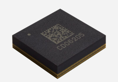
This level of precision is vital for semiconductor applications such as photomasks, lead frames, and microelectromechanical systems (MEMS), where maintaining exact specifications can make all the difference in performance. The process is also well-suited to fabricating shielding components, sensors, and precision connectors — elements critical to ensuring the reliability of semiconductor devices.
In an industry where speed and cost control are paramount, micrometal Group’s PCE process offers distinct advantages. Unlike traditional methods such as laser cutting or stamping, PCE doesn’t rely on expensive tooling, making it an economical choice for both prototyping and full-scale production. “One of the reasons PCE is gaining traction in the semiconductor industry is its cost-effectiveness,” adds Kern. “We can quickly transition from design to production, reducing lead times while maintaining the highest quality standards. This gives our customers the flexibility they need to innovate without breaking the bank.”
Because the process can be adapted for both small batch and high-volume production runs, it provides flexibility for semiconductor manufacturers at various stages of product development. Whether it’s a small run of highly specialised parts or mass production for global distribution, micrometal Group’s PCE process offers a scalable solution.
CPU computer (central processing unit) on circuit board background. US vs China chip war or tech war, semiconductor industrial competition concept. US restrict and control chip export to China.
As semiconductor components continue to shrink in size while increasing in complexity, manufacturers need a reliable production partner capable of delivering consistent, high-quality results. The applications benefiting from micrometal Group’s PCE extend across multiple sectors, from consumer electronics to automotive and aerospace.
Kern concludes, “The semiconductor industry thrives on innovation and precision, and our PCE process is a perfect match for that environment. By providing a highly accurate, flexible, and cost-effective solution, micrometal Group is helping companies achieve their next breakthrough. Using our cutting-edge PCE process, the future of semiconductor manufacturing looks brighter, faster, and more efficient than ever.”


